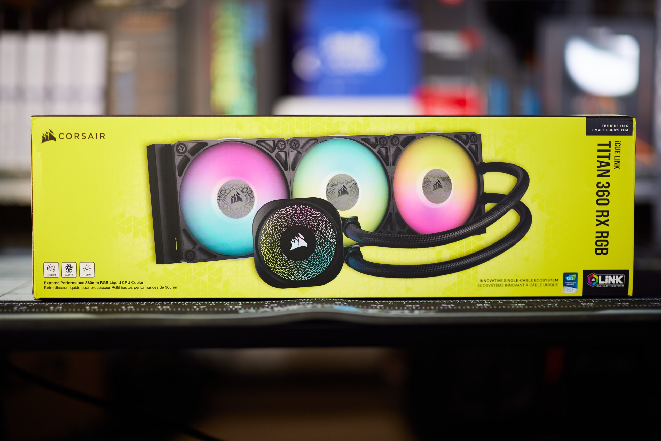
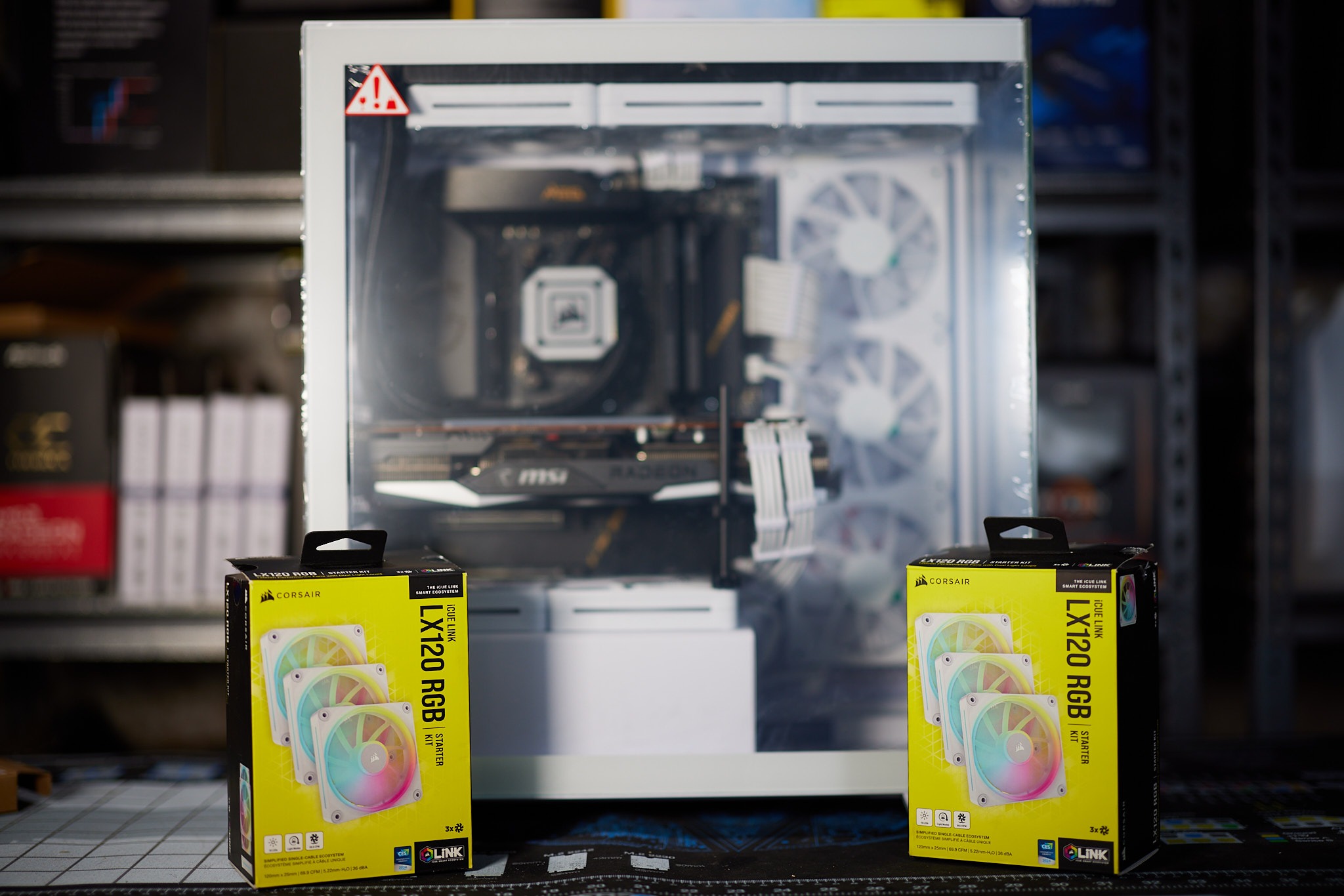
The discussion around All-In-One (AIO) CPU coolers versus custom loops will always be ongoing. However, recently there has been a lot of innovation in the AIO market by manufacturers to try to match the performance and customizability of custom loops. Corsair, not to be outdone by its competitors, is launching its next-generation AIO CPU cooler, the iCUE LINK Titan RX RGB. The Titan combines Corsair's latest advancements in cooling engine technology, replaceable pump caps, and iCUE LINK RX120 fans in hopes of being your next CPU cooler.
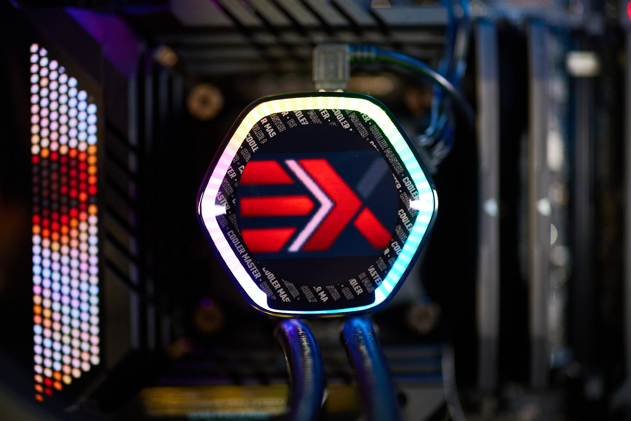
In addition to the Titan AIO, Corsair supplied me with three of its CapSwap modules. This review will examine the iCUE LINK LCD Screen, VRM Fan, and Pump Cap Groove modules. Is the Titan good enough to topple another AIO I've recently reviewed, the Cooler Master 360 Ion? Continue reading to find out.


A CPU or “Central Processing Unit” as we know it in the modern era consist of many parts, some of which you need to know about and some that are things that used to be part of your motherboard which were later integrated into the CPU for efficiency. Read on to find out about the different elements of a CPU and what they are for.
CPU Common Terms
Processing Cores
“Cores” are a basic part of any CPU, the Cores are what handle all the workload. Some of that workload is handed off to their little brothers called “Threads”, which we will talk about next. The main job of your cores is to provide both stability and speed to the processing of data in your PC. They come in many different configurations from both Intel and AMD, depending on processor series and model numbers they differ from the likes of a dual core for light workloads, all the way up to the monsters for special use cases that are 32 and sometimes 64 cores. They all do the same job the same way at different speeds and use different configurations of cores and hardware to interface with the motherboard, Think of a processing core as a piece of silicon that reads 1’s and 0’s at an alarmingly fast rate, and relays that data out to your GPU, hard disk/SSD, RAM, Etc.
Threads
Threads were introduced in the early 2000s when Intel released the “Pentium 4 with Hyperthreading”, The premise of threads is very basic, it divides the load handed to the core in half and hands it off to 2 worker threads inside each core, therefore processing data faster. Threads are that second thing you’ll read on every CPU box you pick up at your local parts store, and they are normally double the count of cores on a CPU. Say you pick up a CPU that is 6 cores, more often than not it will also list as having 12 threads on the box as each core has 2 threads.
IMC
The IMC or “Integrated Memory Controller” controls the communication between the CPU and RAM mostly, but also talks to other parts of your PC, like your hard drives or SSDs to fetch data for the CPU to process, and to your GPU to offload that data from RAM to be rendered on your screen, it plays a key part in how your system operates, That’s why you hear so many people on enthusiast forums talking about avoiding high voltages to reduce chances of damaging the IMC, if it becomes damaged you lose function of some RAM slots or “channels” on your motherboard thus reducing your max memory capacity, permanently.
Chiplets
The chiplet design has become a more recent way to pack many cores together in one space, for example AMDs chiplets are up to 8 cores and 16 threads each, and multiple of them can be assembled onto one CPU “package” or “substrate”, providing larger core counts for ever increasing workloads in a smaller amount of space. The density is what makes this so easy to scale up for manufacturers. Put simply, Chiplet designs allows you to pack in more cores onto a CPU.
Substrate
This is the thing you hold with your fingers when placing the CPU in its socket, and is also what all the connections from the CPU to the motherboard is part of, this magic piece of engineering allows all the cores and threads to talk to each other and the rest of the computer via the motherboard to make everything operate.
ALU
The ALU or “Arithmetic and Logic Unit” is what modern CPUs use to process mathematics efficiently, simply put any math you do on your PC runs through this unit, everything down to simply using the windows calculator function, this removes stress from your cores to do other operational procedures for your PC and also spits out results in a very timely manner.
Cache
All modern CPUs come equipped with cache, commonly referred to as L1, L2 or L3 . L1 cache is a set amount linked to each core and cannot be accessed by other cores for use, this is great for multithreaded processes as each core will get assigned a job in order as it finishes its previous. L2 and L3 cache differ in two ways, L2 cache is usually shared between a “cluster” of cores, 4 cores at maximum normally and they can communicate with each other via this L2 cache. L2 cache is much larger than L1 cache, but is usually half that of L3 cache. L3 cache is shared by the entire CPU for incoming and outgoing data, it is the data flood gate if you will, constantly feeding each other level of cache all the work to do while your PC is on, keeping your cores and threads hard at work.
There are different cache types, L1,L2 & L3 and they differ in cache size and operational speed. L1 is the fastest of the lot, but has the lowest cache so far as size in the region of 1MB. Next you have L2 which has a larger cache in the region of 8MB which is more than L1 but it is slower. Lastly you have a L3 which will have the largest amount of cache in the region of 64MB. While L3 Cache is far larger in size and is able to store far more data, it is also the slowest of the bunch.
FSB
The FSB or “front side bus” controls the speed at which you RAM sends your CPU information, normally measured in MHZ most commonly. This controls the rate at which data is processed. The faster it gets loaded into your CPUs cache, the faster it gets processed.
Lanes
Lanes are used in CPU jargon all the time, they’re all over spec sheets and motherboard sheets, but what are they really? Put simply. A x1 PCI-E slot transfers data via 1 data path to the CPU, which is very slow and rarely used in modern times. x4 PCI-E slots have 4 data channels connected to the CPU providing 4 times the data bandwidth or transfer speed if you will. The same terms carry to x8 PCI-E slots and x16 PCI-E slots. On some cheaper motherboards, some of these lanes will be controlled by a “southbridge” which is a chip that communicates with a CPU at a slower rate than those of direct connections. It is not very noticeable until you get into situations that need those lanes to be direct, like GPUs or you sacrifice performance. Each CPU is only given so many lanes for these data interactions, so eventually you will run out if you have too many devices installed. It is worth noting that any device that utilizes the PCI-e interface will utilize CPU lanes, this includes storage devices such as NVMe drives.
Clock Speed
Clock Speed determines how many instructions per clock cycle, clock cycles are measured by how much data a CPU can process in 1 second. say your CPU is 400MHZ , it would complete 400 million instructions per second. If your CPU is 3.2GHZ it would complete an amazing 3.2 BILLION instructions per second. This speed has climbed over time, as the world has become ever hungrier for faster and more powerful CPUs and the companies manufacturing them are forever pushing the speed limits higher.
Instruction Sets
Instruction sets are what make a modern processor tick, and do its work in different ways as to optimize speed and efficiency, ill give basics of what each one does here, as if I went into full detail this would be several pages in length.
MMX
MMX is intel’s first MAJOR instruction set change, arriving with Pentium 2 and still used today. MMX is used for unpacking data in order at a faster rate then normal I/O Speeds once it is in a CPUs cache, It is however limited to 32 bits of unpack because it was designed as an x86 instruction set.
SSE2/SSE3/SSE4
These three instruction sets share a name and an exact replication of functions, other than bit size increases as newer processor architectures hit the market as x64 instead of x86 instructions, the basic premise of SSE since its birth was floating point integer calculation, the number value getting a larger theoretical maximum at each iteration along the way, SSE4 topping out at 128 bits of floating point activity at once, the former SSE2 being only 32 bits at release.
AVX/AVX2
AVX and AVX2 do floating point vector calculations, the former being limited to 64 bits and the latter boasting a massive 256 bits of data crunching AVX was designed for the long data code lines of modern programs today, it is mostly showcased in video encoding and editing software.
AMD-V
AMD-V is well, AMD’s instruction set for virtualization, it is quite a bit more complex than most think. With it disabled in the BIOS a virtual machine will not run on your system as the hardware acceleration required will not be available.
Intel VT-x
Intel’s VT-x is the same thing as AMD’s counterpart above, again, with it disabled in the BIOS a virtual machine will not run on your system as the hardware acceleration required will not be available.
NOTE: THE LIST OF INSTRUCTION SETS LISTED IS NOT EXHAUSTIVE, ONLY THE MOST COMMON WERE EXPLAINED IN MINOR DETAIL.
CPU Building Blocks
Die Lithography
I know the above name sounds like the name of some cheap book, but let me explain there’s quite a bit to this. You see the NM arms race in the CPU world is partially driven by this, die lithography is the overall size of the CPU die without the heat spreader also referred to as an IHS. Measured in millimetres Squared, for example intel’s current die size for their six core core is 180MM squared, whereas AMD’s current die size for 8 cores is 80.7mm squared, this is due to different lithography’s being used. Namely Intel uses what is called a “monolithic” die lithography, which means they pack everything they can into one chip all connected to each other usually causing the heat output to be focused to the central area of the heat spreader. AMD however uses a “chiplet” type lithography, separating sets of cores and the I/O die from each other into their own separate chips, and spreading them out upon the substrate, this means that generally the heat output to the heat spreader is more evenly distributed.
Die NM (Nanometre) and what it means
When you hear the technology news say “so and so company is moving to a 7NM process” its based on an old measurement that has been used for a long time, the NM figure in chip manufacturing refers to the gap between transistors inside the CPU Die, for example back in the early 2000’s we had 65NM, which compared to todays 7NM spacing is quite a big leap in closing the gap. The smaller the gap (essentially wasted space), the more space that is then created to house more transistors and ultimately allows CPU manufacturers to create more efficient/powerful CPU’s. Competition is fierce between the likes of Intel and AMD as to who can get to the next smallest NM iteration and can be the difference as to who wins the CPU performance crown at any given time.
Main Players In The Industry
Intel
Intel has been around since the late 60s, 1968 in fact. They originally made processors such as the the 4004 for use in complex commercial calculators, the invention if the microprocessor was pioneered by Ted Hoff, one of the founding 8 men of Intel back then. This breakthrough didn’t hit until 1971, it took years of engineering to get that far, but intel soon stormed the world with their invention, it was in such demand they needed 3rd party manufacturers to make enough to keep up with the demand. Which is ironically where their only competitor originally started off from.
AMD
AMD, or Advanced Micro Devices started up in early may of 1969 as a 3rd party manufacturer of Intel’s 4004 microprocessor. Intel also licensed them all of the schematics and specifications to produce the product, later on in 1971 AMD produced its very first processor of its own, the AM2501 Logic Processor. The rivalry of the two companies began then, and is still in effect today.
Strengths And Weaknesses
There is the age old question, “who is faster than who” when it comes to Intel and AMD, but I will point out what each is good at from a general standpoint. In the end, you, the end consumer has the choice to make depending on your use cases, The list below sums up both sides of the fence, short and brief.
Intel
As of this article’s writing, intel has the following strengths over AMD:
- Higher Boost Speed Clock
- Gaming FPS (higher than AMD in single threaded games in most cases)
- Faster Single Threaded IPC (Instructions Per Clock)
And the following Weaknesses, Compared to AMD:
- Increased operating temperatures
- Multithreaded workloads
- Power hungry
AMD
As of this article’s writing, AMD has the following strengths over Intel:
- Multithreaded workloads
- Video Encoding
- Streaming
- Core Count
And The Following Weaknesses, Compared to Intel:
- Slower Boost Speed Clock
- Gaming FPS (lower than intel in single threaded games in most cases)
- Slower Single Threaded IPC by a very small margin (Instructions Per Clock)
Summary
This about sums up the basics of what makes up a CPU in 2022. As with most topics, you could really go in-depth. CPU’s are no exception to this rule due to their shear complexity. However I hope this article give you a basic understanding and somewhere to start.
As always, if you enjoy my writing, feel free to let me know.
This Post Has 3 Comments
Leave a Reply
You must be logged in to post a comment.


It’s about time I learned what all that meant! This is the best piece of literature you’ve ever written Jay.
very funny Odacava
10/10 😀