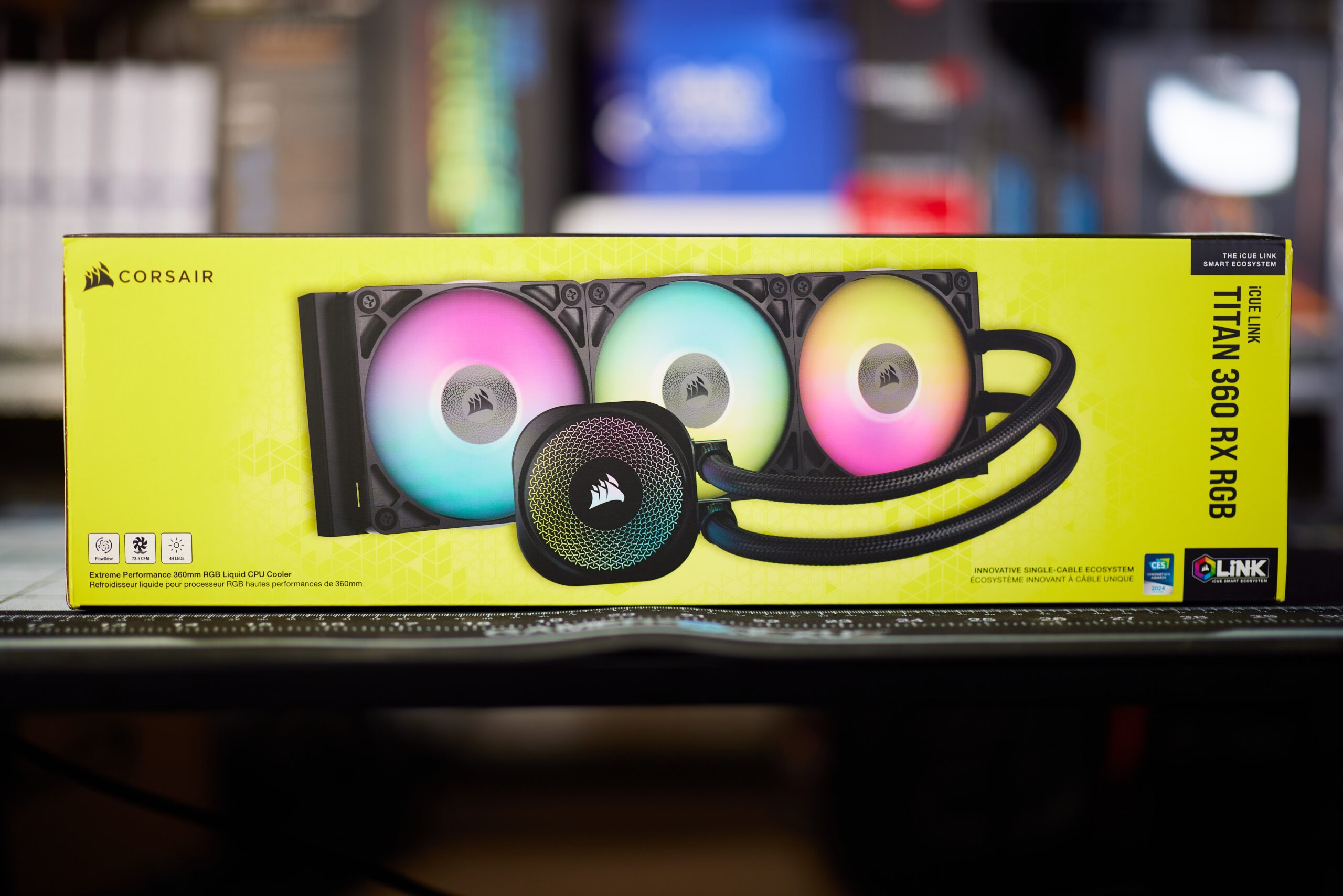
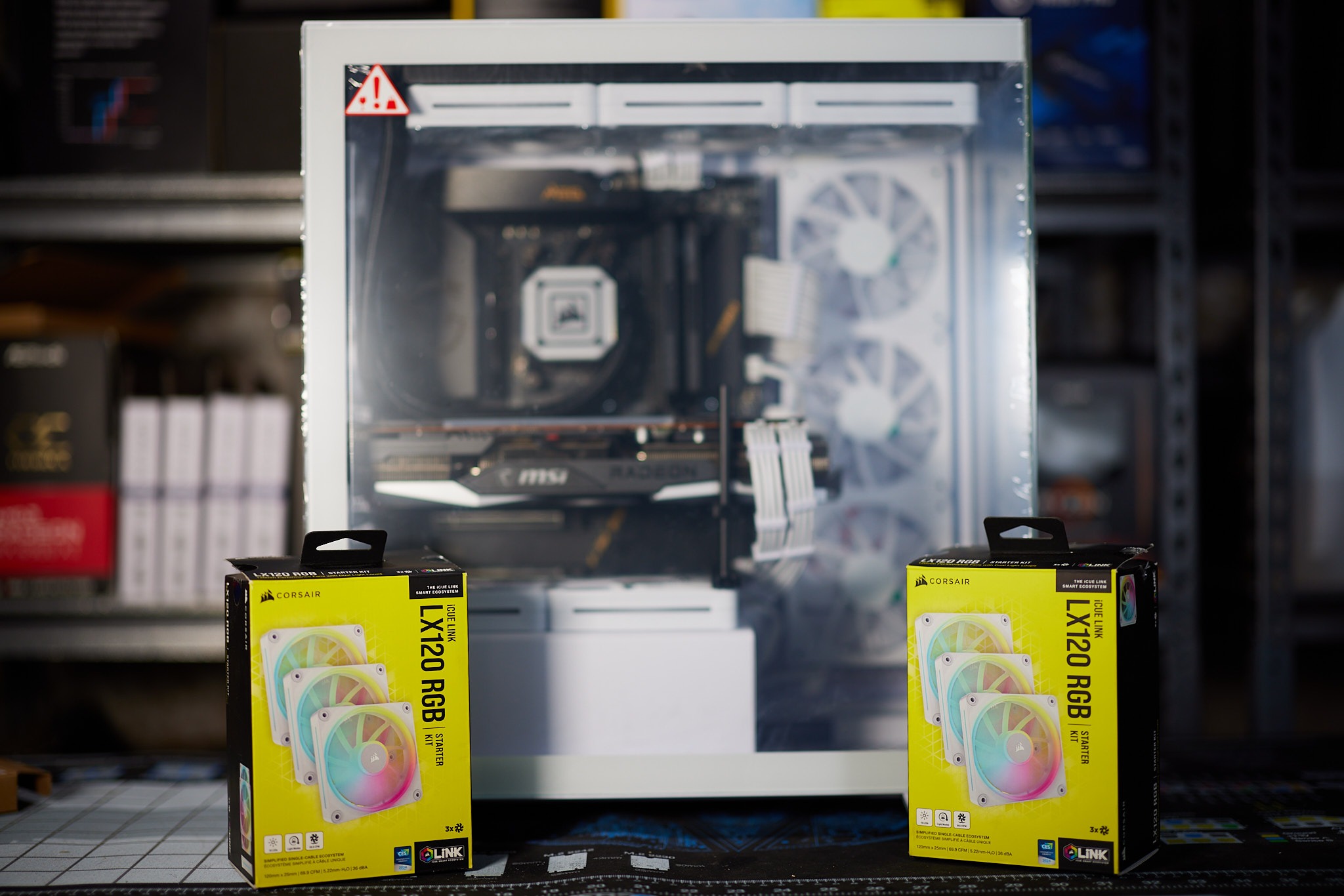
The discussion around All-In-One (AIO) CPU coolers versus custom loops will always be ongoing. However, recently there has been a lot of innovation in the AIO market by manufacturers to try to match the performance and customizability of custom loops. Corsair, not to be outdone by its competitors, is launching its next-generation AIO CPU cooler, the iCUE LINK Titan RX RGB. The Titan combines Corsair's latest advancements in cooling engine technology, replaceable pump caps, and iCUE LINK RX120 fans in hopes of being your next CPU cooler.
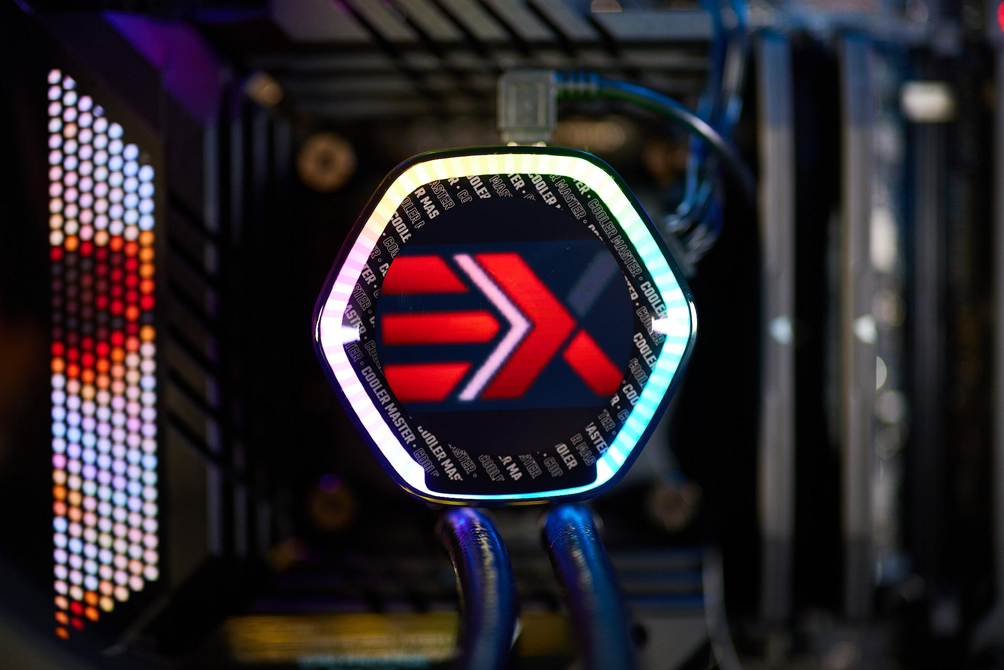
In addition to the Titan AIO, Corsair supplied me with three of its CapSwap modules. This review will examine the iCUE LINK LCD Screen, VRM Fan, and Pump Cap Groove modules. Is the Titan good enough to topple another AIO I've recently reviewed, the Cooler Master 360 Ion? Continue reading to find out.


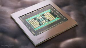
If this is your first time joining the PC building space, you may be wondering what we refer to as a “GPU”.
GPU is short form for “Graphics Processing Unit” its that lovely thing you plug your monitor into to see your computer’s screen and play all your games on, and depending on how powerful it is, it can effect how games look visually and also how they run. Let me give you a simple history of the big players and effective breakdown of how this process works.
Life for GPUs started back in the early 90s they were a much simpler form of what they’ve become today through advancements. But, to touch on the “magic” of how a GPU works, let me explain the basics. A GPU is comprised of 3 basic things:
- Processing Unit
- VRAM
- Interface
A few of these things have evolved and changed over the decades, but ill stick to the most recent iterations to save you a long and boring 30 year history lesson.
Processing Unit
The Processing Unit or “brain” of a GPU is what renders what’s on your screen, it is essentially a giant overpowered calculator that takes in the case of games “frames” like pictures for example, so many 10s or hundred of “frames” are processed per second to give you movement in your game that is free flowing, these pictures are sent to it by your CPU, which reads data from your HDD or SSD, and relays it to this unit to make the picture or “graphics” on your screen. There are different types of processing units referred to as “cores”, we will get into this once we get company specific later on.
We all know about RAM in a computer, but what makes VRAM special for a graphics card?
VRAM
VRAM or “Volatile Random Access Memory” is a special kind of memory used on on GPUs, mainly for its speed of read/write functions it is “volatile” because unlike your system’s RAM, it is wiped many times per minute and if it starts to “go bad” or “wear out” artifacting occurs on screen, usually in the form of unwanted colored squares, or sometimes a completely green screen and no picture.
Getting more in depth with VRAM or “GDDR” as its referred to, the long form of this name being Graphics Double Data Rate, it is specific to GPUs and has a different design than your system RAM. The most coming today are GDDR5, GDDR5X and GDDR6 their expensive bigger brother. The difference between the 3 of these is memory clock speeds, and data transfer rates, along with voltage requirement decreases. GDDR5 has a max theoretical throughput of 338 GB/s at a clock speed of 7Gbps on a 384 bit memory bus using 1.5v to run the memory modules, therefore making a GPU slightly more power hungry. GDDR5X was the “half way step” of improvements before GDDR6, increasing throughput to a max theoretical output of 528 GB/s and a clock speed of 11Gbps on a 384 bit memory bus using only 1.35v, thus lowering power demands and increasing performance. But was also very costly to make at the time, so not man GPUs saw this version unless they were very high end.
GDDR6 is the current king, with a max theoretical throughput of 672 GB/s and a clock speed of 14Gbps on a 384 bit memory bus, using 1.25v to power the memory, thus making it the most efficient and todays GPU memory standard until we move further along in technology.
Interface
What is an interface you ask? When you take a GPU off the shelf in the store it says things like “PCI-E 3.0” or “PCIE 4.0”or even “PCI-E 5.0” on the box, this is the type of interface and rated speed it requires to operate properly PCI-E or “Peripheral Component Interconnect Express” is the spot on your motherboard the GPU fits in to, it allows the sending of data and power to the processing unit and VRAM. Therefore allowing your PC to render a picture on your monitor if its plugged into the GPU.
These three versions of PCI-E have different specifications, but the newer versions are backwards compatible with older cards, so there is no worries there, so lets talk about these differences. PCI-E 3.0 is now much older but is a stepping stone so we’ll start there a x16 lane of PCI-E 3.0 (that long slot you put your GPU into on your motherboard is this lane) has a max transfer rate of 8.0 GT/s, the number for the the max throughput on an x16 lane being 15.754 GB/s of data, PCI-e 4.0 improves on this number by doubling it, with a max transfer rate of 16.0 GT/s and max throughput being 31.508 GB/s, it is backwards compatible with PCI-E 3.0, slowing itself down automatically to match the older technology. PCI-E 5.0 is the latest big kid on the block as of 2022, again, doubling our numbers with 32 GT/s transfer rates and max throughput being 63.015 GB/s PCI-E 5.0 is fully backwards compatible with both of its slower brothers, again slowing itself down to match speeds with the GPU installed.
Now to get on to the companies who make GPUs, there are really only 2 major players left in this space AMD and NVIDIA each company has its relative strengths and weaknesses and its own special feature set you have to decide which you like, a lot of peoples minds change over time, trust me on this one.
Nvidia
NVIDIA is what many people would deem the “premium” brand of the two, their cards almost always cost more than their counterparts, and they rely more on raw performance than any kind of software enhancements. They have their own versions of GPU cores as we discussed earlier, so lets get into them here.
- CUDA Cores
- TENSOR Cores
- RT Cores
Beginning with CUDA cores, Nvidia’s oldest of the 3 technologies, what is a CUDA core you ask? CUDA stands for “Compute Unified Device Architecture” it is a name given to the parallel processing API or software that is proprietary to NVIDIA, and is a little less work in some ways for game developers, they can code its instructions on C or C++ and it will read them, thus allowing them to work around other pieces of software. Namely DirectX and Open GL. The CUDA cores are NVIDIA’s horsepower if you will, they pack more of them into a card with each passing iteration, the more they get in there the faster the framerate moves because it becomes effortless for the GPU to process data.
TENSOR cores are a different story all together, you may have come across this term if you’re into AI/Machine Learning. There is plenty of confusion surround how they work, so ill try to explain this as simply as I can. In short tensor cores speed up the process of matrix multiplication, it’s a technology specific to NVIDIA, and is mostly found in its Quadro RTX and TITAN GPU lines for professional space use, it is not really designed for consumers or gamers, thus we will probably never really see it in action in their consumer GeForce line-up.
RT cores or “Raytracing cores” are NVIDIA’s newest eye candy technology, and they tout it as the best thing for gaming, lets look at how these actually work shall we? RT Cores are accelerator units that are dedicated to performing ray-tracing operations with extraordinary efficiency. Combined with NVIDIA RTX software, RT Cores enable artists to use ray-traced rendering to create photorealistic objects and environments with physically accurate lighting. This normally comes at a performance cost in the FPS area of games, to create more eye candy, a lot of users still turn Raytracing off, as they would rather have higher framerates.
NVIDIA carries the following features on its cards:
- DLSS
- PHYSX
- Raytracing
All three of these features have their use cases, the middle child being a much rarer option in select titles these days and has become more of a marketing gimmick than anything. But let me explain what each of these features do, starting with DLSS.
DLSS or “Deep Learning Super Sampling” as its extra long name implies, is a hardware-based AI software controlled “math problem” if you will. It allows you to upscale a lower screen resolution to a larger one, at the cost of graphic fidelity for FPS or “frames per second” in a game title. The larger the FPS count, the smoother the gameplay so in some games this is an advantage. However, if you would rather the game world look amazing as the game is more cinematic (i.e Tomb Raider, Horizon Zero Dawn) then I would stay clear of this option, as these type of games do not so much rely on FPS for a gameplay experience, but rather the atmosphere. DLSS is proprietary, and only works on NVIDIA GPUs. It also must be implemented by developers on a per game basis.
PHYSX is a much older technology that NVIDIA acquired by buying out a smaller company named AGEIA in the 90s, it is essentially a hardware based physics engine, allowing a slightly “lazy” or “cheaty” way for a game developer to implement features in a game that require physics, for example, the flying dirt and car impact damage mechanics in a rally racing game, or much simpler, the hair on characters in a video game moving with the wind and moving with their body movements. PHSYX is a rarely used feature these days, and if a game company uses it they almost always advertise it being in their game, it is another NVIDIA proprietary piece of magic, but their competitor is slowly figuring out how to implement their own way of making those calculations.
Raytracing is NVIDIA’s latest advancement many simply refer to it as “the tracing of rays”, raytracing employs dynamic lighting in video games and makes it look as real as possible, but it also comes at a big FPS performance hit for their lower to mid tier GPUs, which most turn their nose up at and disable it for this very reason, though for some games as mentioned earlier, the visuals are worth this cost. In anything competitive, raytracing can hurt you big time.
AMD
Now on to the competition, AMD or as most used to refer to them the “underdog” of the graphics world. AMD acquired a now dissolved company named ATI back in 2006 who used to be NVIDIA’s competition, and has been a more price to performance ratio based company since then, offering slightly less or equally powerful GPUs at a lesser cost AMD makes their GPUs enticing this way to a new builder, and they are not a slouch in performance by any means, In recent years AMD has caught up in the performance part of the market, breaking even or being just slightly behind their competition in benchmarks, their pricing is still effectively lower. The biggest key with AMD is their cards’ software suite, it jumps ahead of its competition in this manner, adding more features this way instead of hardware locking them. They are also reputably open source, to the cheers of the growing Linux community, lets get into the grit of AMD here.
- Compute Units
AMD’s compute units are essentially the same thing as NVIDIA’s CUDA cores, just without the fancy moniker and no proprietary lockdowns, these are the horsepower of AMD cards they are improved upon and multiplied with each new GPU core released, increasing performance drastically. Their parallel processing API is much more streamlined and open source coded. They freely supports Open GL and DirectX, along with the freedom for Linux users to compile their drivers for use on an operating system other than windows.
AMD carries the following features:
- FFSR
- RSR
- SAM
- Infinity Cache
FFSR or “FidelityFX super resolution” is AMD’s answer to DLSS, it is however open source and works on both AMD and NVIDIA GPUs, but it must be implemented by game developers on a per game basis, just like its counterpart it “upscales” or “super samples” a lower game resolution up to a bigger one to increase FPS at the cost of visual quality in game. As with DLSS the same issues apply here, although AMDs version can be called a bit more polished. Both have a visual fidelity disadvantage to running “native” screen resolutions.
RSR or “Radeon Super Resolution” is something new on AMDs bag of offers, only released recently it has a distinct advantage to those who wish to use FidelityFX, in that RSR is FidelityFX but it works in any game available on the market, because it is a driver controlled version of FidelityFX, the downside here is again, it lacks a tiny bit more visual quality than FidelityFX, as its not specific to any given game, or coded as part of the games it gets used on. Those who already use FidelityFX will not notice much of a difference, if any.
SAM or “Smart Access Memory” is a very cool hardware feature AMD implemented on its latest GPUs, it allows the CPU in your PC direct access to the processing unit on your GPU, therefore increasing data transfer speeds and usually FPS in most games.
Infinity Cache, unlike its name it does not scale to infinity and beyond (bad toy story reference I know), but it is sort of magical in its own way. Infinity cache scales memory bandwidth dynamically, allowing increased memory access speeds and normally increased framerates, though in some use cases it really doesn’t do much.
In Closing
With what I have explained for you here, I hope you now understand how your GPU works and who your options are as far as companies and features, who you chose to purchase will usually squarely lie on who you want to try, what your requirements are, and more importantly your budget is to build your PC or upgrade it. Pricing has its highs and lows when it comes to PC components, but especially GPU’s as they have a variety of uses, which includes mining and other such activities. As we have seen recently, there has been huge demand for GPU’s due to mining which pushed prices through the roof. So remember, sometimes it is better to wait for prices to come down instead of throwing your hard earned money away at artificially high prices. Good luck in your GPU adventures!
This Post Has 5 Comments
Leave a Reply
You must be logged in to post a comment.


Well done sir! Your Latino Ron Jeremy avatar is questionable.
I am sorely tempted to create a faux account and start asking him about the AGP on “my grandma’s Dell”, circa 1995.
Awesome article man, good job!
Very well written and nicely explains the subject for those of us who have been using cards for years and also for those who may be looking for information before making a first time purchase. 🙂
I am a GPU!