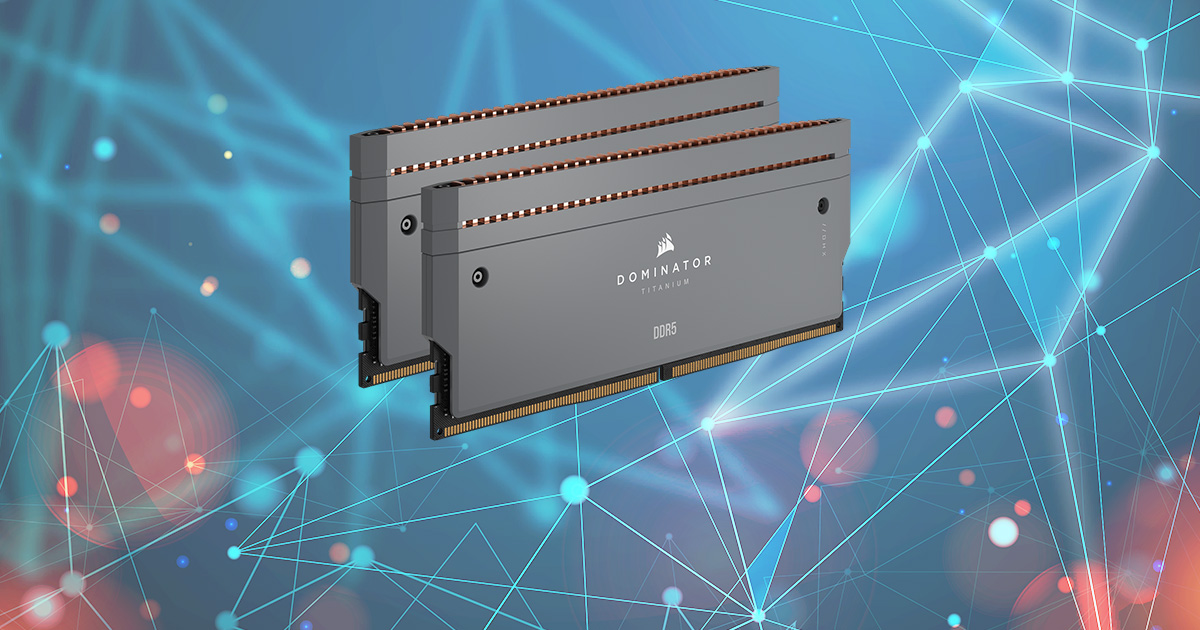
Similar to the launch of Ryzen 3000 series, the newly released Threadripper 3 series introduces greatly enhanced memory overclocking capabilities. To test out these new overclocking capabilities, Corsair sent us a kit of their popular Vengeance LPX DDR4 memory modules. Using the new Threadripper 3970X CPU, we will evaluate the performance of this memory and investigate its strengths and weaknesses. Originally intended for Intel platforms, the Vengeance LPX will be put to the ultimate compatibility test on the TRX40 platform.

Since they were founded in 1994,
CORSAIR has grown from pioneering the high-performance DRAM market into one of the worlds leading providers of high-performance PC peripherals and components. CORSAIR offers a complete range of products to equip gamers, enthusiasts and e-sports athletes, including mechanical keyboards, precision gaming mice, wireless headsets, high-performance components that gamers use to build gaming PCs, and the CORSAIR ONE fully-integrated gaming PC. With a company-wide commitment to quality, innovative design, advanced features and high performance, CORSAIR products have won thousands of media and industry awards, earning their place in gamers hands and PCs following years of development and engineering by a team dedicated to building great products they themselves would want to use. -Corsair
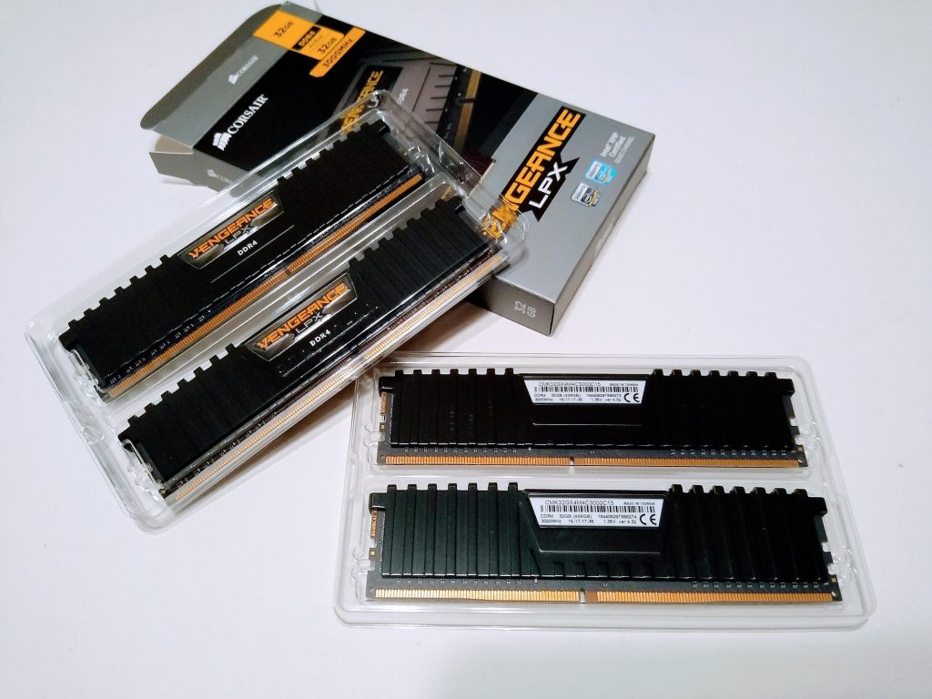
Designed for high-performance computing and computer enthusiasts, Corsair offers a truly dizzying array of options. The Vengeance LPX memory modules come in densities of 4GB, 8GB, and 16GB.
In terms of frequency and latency options it starts with the humble 2133 MHz CL13 and goes all the way up to the mind-boggling 5000 MHz CL18. All told, there are 25 different frequency and latency options to choose from. When it comes to kit combinations, Corsair doesn’t disappoint there either. The Vengeance LPX comes in 18 different density configurations ranging from a 4GB single stick all the way up to a 128GB kit composed of 8 x 16GB sticks.
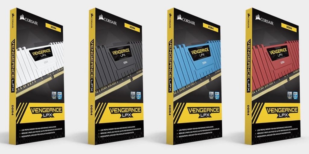
Take the already monstrous product line and multiple it by four, as Corsair also offers the Vengeance LPX in four different colors consisting of white, black, blue, and red.
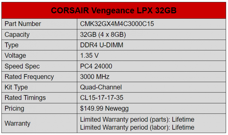
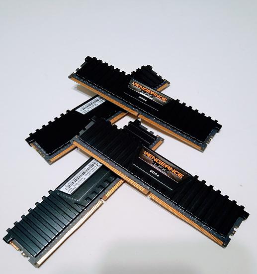
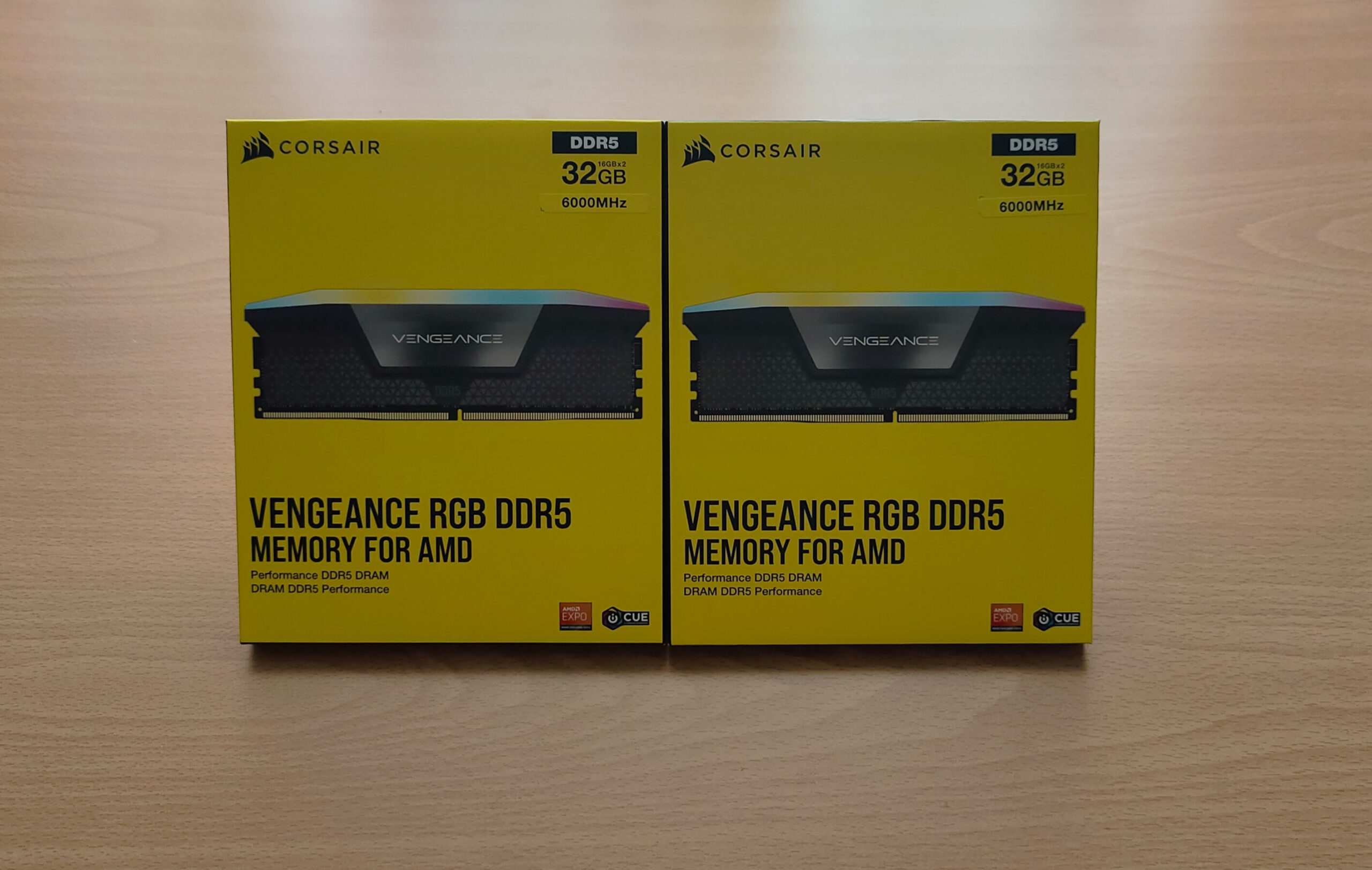
Today we are evaluating the 4 x 8GB kit of 3000MHz CL15 memory, in black.
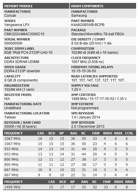
Below is a screenshot of Thaiphoon Burner, which is a free tool that allows one to read the Serial Presence Detect (SPD) firmware of the DRAM. The SPD information is critical in determining how the stick will perform and how the computer will recognize it.
As the Thaiphoon Burner screenshot shows, this specific kit of memory is composed of Samsung B-Die ICs. Each memory module uses a total of 8 ICs, all of which are located on only one side. As you might know, Samsung B-Die has become synonymous with high frequency and tight timings. Overclockers, gamers, and system builders alike all flock to memory composed of Samsung B-Die ICs. They have become the gold standard to which all other memory ICs are compared.
That being said, this is the lowest XMP bin of B-Die we have ever seen. We theorize that this kit is running the OEM version of B-Die, which is seemingly different and doesn’t have the aforementioned attributes for overclocking. Later on we will explore the overclocking capabilities so follow along if you would like to see more.

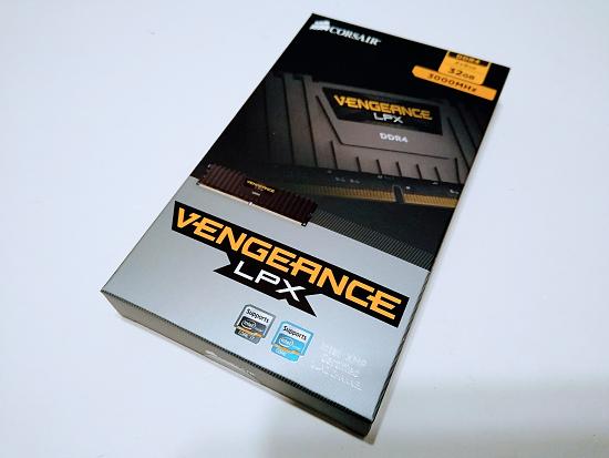
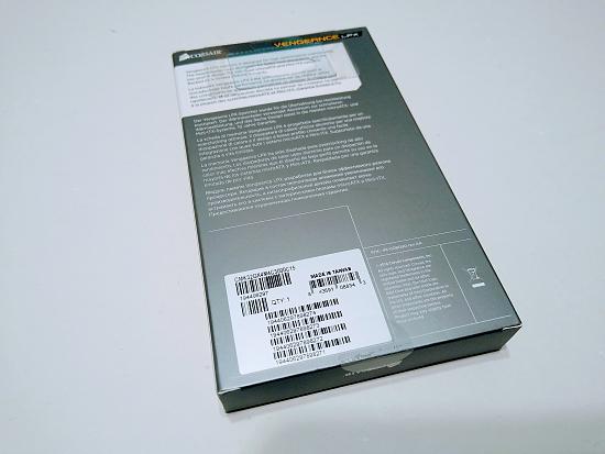
Packaging is often overlooked. It serves the function of safely shipping the product, but also as a first impression of the overall quality. Corsair ships the Vengeance LPX in a simplistic box and clam shell design.
Inside the box, the memory modules are safely tucked away in two plastic clam shells. It’s certainly not an elaborate packaging, but it is effective and ultimately saves you money in the end.
The outside of the box tells us that this memory was designed for Intel platforms with the Intel XMP branding and logo’s. This might pose an issue because we are testing this memory on AMD Threadripper 3.
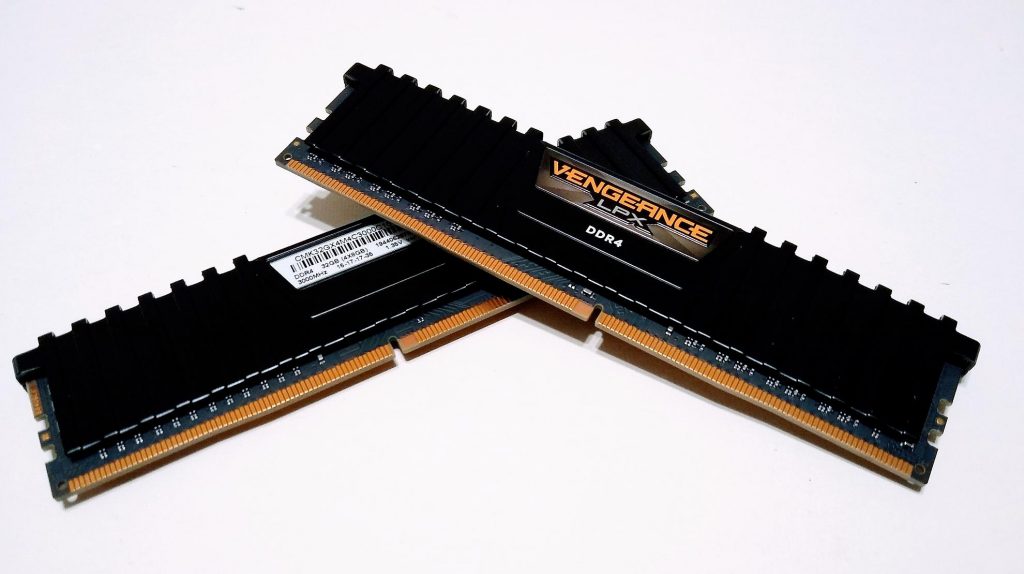
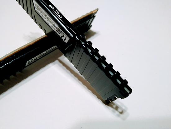
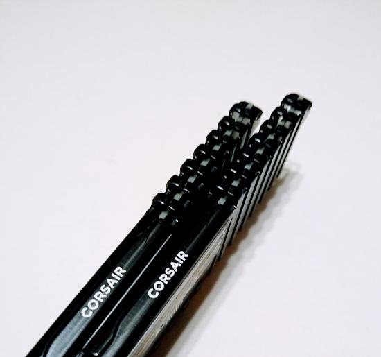
Our first look at the memory we see the all-black aluminium heat sink. The overall size is quite low profile and doesn’t protrude much beyond the actual PCB itself. The memory module has a lightweight feel in hand but the aluminium feels sturdy.
Samsung memory has been known to produce moderate heat for memory. Within the XMP 2.0 voltage limit of 1.50v, the typical heat output is just a few degrees Celsius above ambient. Although the heat sink is on the small side, we believe it will be very effective at dealing with the nominal heat output.
The styling is subtle but makes a definite statement. Our review modules have a classic glossy black appearance which should make them match other system components.
The potential upside to low-profile memory heat sinks is that they will not interfere with the CPU cooler. This is something that first time builders and beginners often overlook, but tall memory heat sinks can conflict with some large aftermarket CPU air coolers.

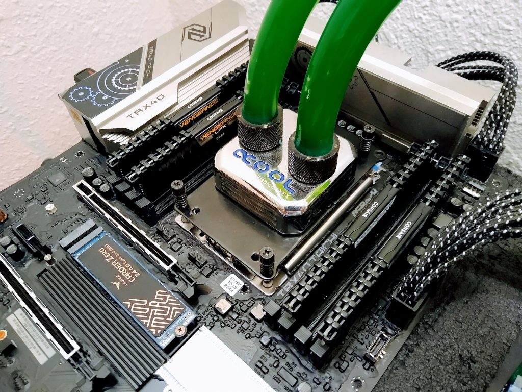
Installed in our test rig, the Vengeance LPX makes quite an attractive paring with the ASRock TRX40 Taichi. In this case the heat sink size and profile was not an issue because we are using water cooling.
The overall objective is to evaluate the memory from the perspective of daily usage. We will try to answer the question of what memory speeds produce the best results for overall performance and productivity. The approach is to first test the XMP 2.0 profile. Once we have established that the XMP profile is working on the test system, then the real fun begins as we evaluate the memory from an overclocking perspective.
Additionally, we will briefly examine how Ryzen Threadripper responds to memory overclocking and examine what types of overclocks can be carried out with reasonable voltage levels. To accomplish this task, we will turn to benchmark programs to examine the performance of the memory and overall system under various conditions.
XMP Profile
The XMP profile for this memory was intended for Intel platforms, as is stated on the outside of the box. We know that AMD platforms require slightly different DDR4 timing profiles than the Intel counterparts. So the first test is just to apply the built in XMP profile, and see if it the system even boots at all. If the XMP profile is able to be set in the bios then we will enter the OS and stat testing.
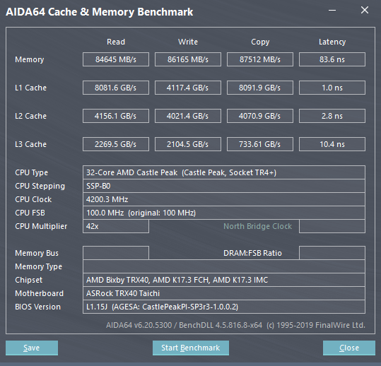
Given the the profile speed is running a modest 3000 MHz, we didn’t have any issues with the XMP profile. It quickly and effortlessly trained all the profile timings in the bios and once in the OS, everything was rock solid stable. However, as soon as we got to the OS we soon realized that all of the monitoring software showed CL16. We double checked that the motherboard was still set to CL15, so there is an issue with the AMD platform at the moment.
We tried a different kit of memory and confirmed that it’s a platform problem and not a problem with this memory.
FCLK = 1800 MHz; UCLK = 1800 MHz
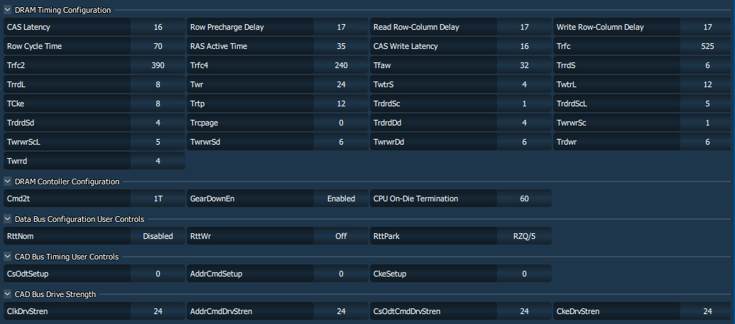
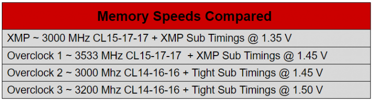
Overclock 1 ~ 3533 MHz CL15-17-17 + XMP Sub Timings @ 1.45 V
Once the XMP profile has been successfully tested, we can dive into overclocking. The methodology is to set our maximum working voltage of 1.50 V, to see what could be accomplished, and then lower the voltage to find the stability point.
For the first overclocking attempt, we raised frequency and voltage only and left everything else set by the XMP profile. Due to the fact that our test kit is composed of Samsung B-Die IC’s, we had exceptionally high hopes for this memory. We soon found out that seems to be it’s B-Die in name only and does follow the same overclocking characteristics of other B-Die modules we have tested.
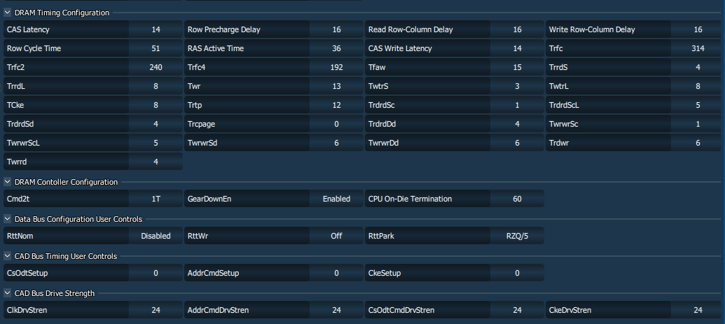
We finally arrived at a frequency of 3533 MHz. That is a substantial 533 MHz over the stock frequency, but it is substantially less than we have seen with other Samsung B-Die based memory models. Below is the resulting timing profile and AIDA64 test.
FCLK = 1800 MHz; UCLK = 1800 MHz
Overclock 2 ~ 3000 MHz CL14-16-16 + Tight Sub Timings @ 1.45 V
The second overclocking test is similar to the first one, but in reverse. In this case we leave the frequency determined by the XMP profile and only adjust the timings. The goal here is to build a timing profile that is tighter and more efficient than the XMP profile, but also one that is fully stable. This can be a lengthy and time consuming process, but there are useful tools to help beginners such as the DRAM Calculator for Ryzen.
In this case we will build our timing profile the hard way, and forgo any timing profile builder tools. Each timing was tested one-by-one to find the optimal balance between stability and performance. As is the case with overclock attempt 1, we found this memory difficult to deal with and not very flexible in terms of overclocking. Below is the resulting timing profile and AIDA64 test.
FCLK = 1800 MHz; UCLK = 1800 MHz
Overclock 3 ~ 3200 MHz CL14-16-16 + Tight Sub Timings @ 1.50 V
The third and final overclocking test is an attempt to combine the first and second ones. In this case we will attempt to build an optimally efficient overclocking profile by adjusting both the frequency and the timings.
We ended up at the same timing profile as overclock test 2, however, we were able to increase the frequency by an additional 200 MHz. Below is the resulting timing profile and AIDA64 test.
FCLK = 1800 MHz; UCLK = 1800 MHz
The heat output of this memory proved to be nominal. With the highest overclocked memory profile, and 1.50 V set in the bios, we observed a scant increase in temperature of 4 degrees Celsius. The temperature was measured by placing a thermal probe directly on the heat sink and recording the temperature with a Fluke 52-2 digital thermometer.
Benchmark programs allow us to examine the performance gain or loss from making changes to the various computer components such as the CPU, GPU, or memory. In this case, the goal is to remove all variables and examine only the performance change from memory overclocks. To accomplish this, all benchmarks were run with the CPU held at a constant 4.2 GHz for every benchmark. We will investigate the effects of memory overclocking not just because it’s fun, but because it has real-world implications and can help with the productivity of daily tasks.
When we go to test the memory and overclocking capabilities we need to take into consideration two new variables: FCLK and UCLK. Even though these variables are somewhat out of our control, they play a huge role in the overall performance and benchmark scoring. That being said, it’s not always fair to compare one frequency against another, because the FCLK and UCLK might be running at different speeds and will, thus, skew the test results. While it’s not within the scope of this memory review to dive deeper into the memory structure, just keep in mind that those variables are there.
First lets examine the memory by using AIDA64 Cache and Memory Benchmark. Specifically speaking,
Memory bandwidth benchmarks (Memory Read, Memory Write, Memory Copy) measure the maximum achievable memory data transfer bandwidth. The code behind these benchmark methods are written in Assembly and they are extremely optimized for every popular AMD, Intel, and VIA processor core variants by utilizing the appropriate x86/x64, x87, MMX, MMX+, 3DNow!, SSE, SSE2, SSE4.1, AVX, AVX2, and AVX-512 instruction set extension. AIDA64
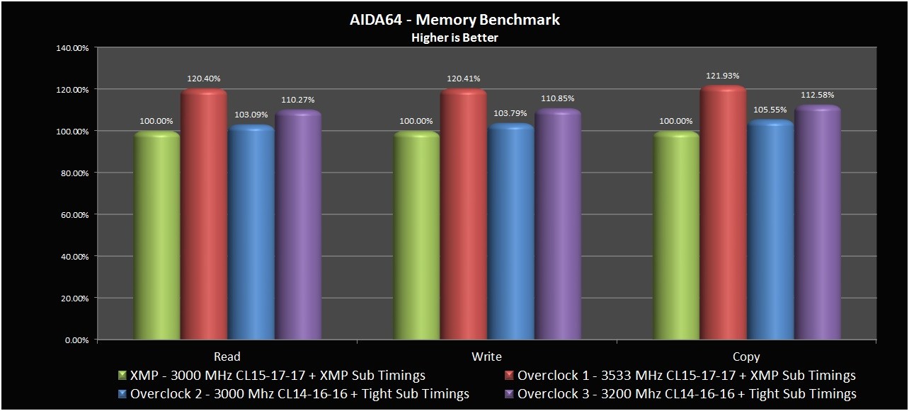
In the chart below, we compare the four different memory speeds and how they affect the overall system performance. As you can see, the first overclocking test case was the clear winner here. Keeping the memory timings fixed by the XMP profile and adjusting the frequency to the max proved to the be best case for all three AIDA64 tests. The results show that AIDA64 clearly favors frequency on this platform.
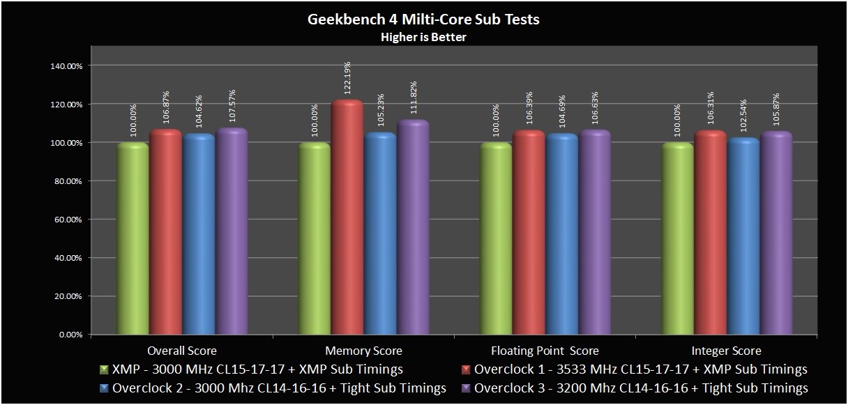
Next up is Geekbench 4. This benchmark utilizes multiple different tests warped into one benchmark, so it’s a great analytical tool to evaluate memory performance. Specifically speaking, it:
Includes updated CPU workloads and new Compute workloads that model real-world tasks and applications. Geekbench is a benchmark that reflects what actual users face on their mobile devices and personal computers. Geekbench
The Geekbench 4 test results parallel the AIDA64 ones nicely with a small difference. In this case, raw frequency overclocking was not the clear winner. Looking at the overall score, the overclock test 1 and overclock test 3 were nearly tied.
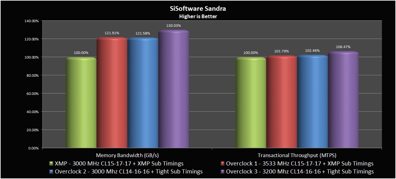
Next, we will examine the performance using a few of the memory benchmark tests offered in the SiSoftware Sandra suite of benchmarks.
SiSoftware, founded in 1995, is one of the leading providers of computer analysis, diagnostic and benchmarking software Sisoftware Sandra.Since launch, SiSoftware has always been at the forefront of the technology arena, being among the first providers of benchmarks that show the power of emerging new technologies such as multi-core, GPGPU, OpenCL, OpenGL, DirectCompute, x64, ARM, NUMA, SMT (Hyper-Threading), SMP (multi-threading), AVX512, AVX2, AVX, FMA3, NEON, SSE4.2, SSE4, SSSE3, SSE2, SSE, Java and .NET. SiSoftware
For both of the tests we ran in the Si Sandra bench marking suite, we found that the combined higher frequency and tighter timings was best.
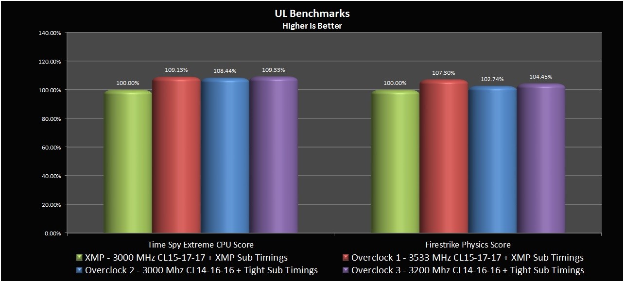
Next we will take a look at two very popular 3D-rendering benchmarks. Specifically, we will look at how the different memory profiles effect the scoring in the Time Spy Extreme CPU score, and Fire Strike Physics Score. Both of those benchmarks are designed to give a real example of 3D performance, but we are focusing on the CPU system performance parts of the test only.
Across the board we saw an improvement in the scores from memory overclocking. This was somewhat an unexpected result because on Intel platforms the gain from memory overclocking in both of those benchmarks is quite small or non-existent.
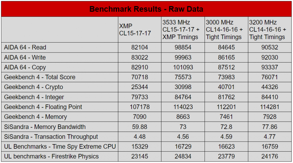
For those interested, here is a table showing all of the hard benchmark numbers from our testing. All of these figures are represented in the graphs above, but we will give you the hard numbers as well.

Overall there’s a lot to love about the Corsair Vengeance LPX. From the simplistic buy tasteful heat sink design, to the staggering array of product options, this memory has something for everyone. While many modern computer builders might flock to RGB memory, the always-popular glossy black design is timeless.
We were pleasantly supervised to find Samsung B-Die lurking under the heat sink. However, once we got into overclocking, we soon realized that there was not as much overclocking headroom as we would have expected. From an overclocking perspective we did manage an increase of 533 MHz beyond the XMP frequency, which is a good touchstone for Samsung memory modules.
With an Newegg price tag of $149.99 they are certainly not the cheapest option available in their class, but they might be the coolest. In terms of competition the G.Skill Sniper X retails for around $115 for the 32GB kit and is running 3000 MHz CL16-18-18. Further competition in the 32GB, 3000 MHz memory field is the Ballistix Sport LT for around $150.
With Corsair’s legendary company history backing them, and given that these our test sample was equipped with Samsung B-Die IC’s, we feel that this kit is an easy win. The modules would make a great addition to any gaming or performance orientated system out there.
Lastly we wish to thank Corsair for providing this memory kit for review ! You can view the kit on Corsair HERE
Want to discuss this product or give your views and feedback from your own usage? Discuss on the ExtremeHW Forums
Like our content? Please consider Donating to help us to continue our writing.


This Post Has 0 Comments